
As electronic devices continue to become smaller, lighter, and more powerful, the demands placed on metal components have increased dramatically. From a metal manufacturing expert’s point of view, chemical etching (also known as photochemical etching or photo etching) has become one of the most reliable and efficient manufacturing processes for producing high-precision electronic components.
In contrast to traditional machining or stamping, chemical etching is a subtractive process in the form of controlled chemical dissolution. And that small difference is just why this process is so well-suited to electronics, where precision, material integrity, and repeatability are paramount.
In this article, we’ll take a look at why chemical etching is the best choice for electronic parts, what benefits it can provide over other manufacturing methods, and how TMNetch chemical etching enables the electronics industry today.
The Unique Manufacturing Challenges of Electronic Components
Electronic components operate under strict constraints. Designers and manufacturers must balance:
- Extremely fine features and tight tolerances
- Thin metal materials that are easy to deform
- Electrical and thermal performance requirements
- High-volume production with consistent quality
Mechanical deformation will be introduced by processes like stamping, CNC machining or laser cutting, and mechanical stress, burrs or heat-affected layers can have negative effects on performance or yield in electronic applications.
Chemical etching addresses these challenges at a fundamental level.
What Is Chemical Etching?
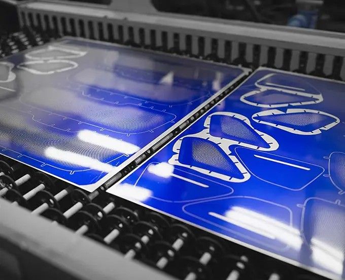
Chemical etching is a type of subtractive process in which an etchant is used to selectively remove metal in accordance with a pattern defined by a photoresist, which is applied as a mask that is transferred from a digital design.
From a production standpoint, the key characteristics of chemical etching are:
- No mechanical force applied to the metal
- No localized heat input
- Uniform material removal across the sheet
- Excellent control over fine details
Because the reaction is purely chemical, the underlying metal maintains its original mechanical, electrical, and thermal properties—something that is necessary for electronic components.
Burr-Free and Stress-Free Processing
One of the most important reasons chemical etching is ideal for electronic components is that it produces burr-free and stress-free parts.
In electronics, even microscopic burrs can cause serious problems:
- Short circuits
- Signal interference
- Assembly issues during automated placement
Chemical etching eliminates such hazards. Edges are smooth and clean, as the material is dissolved and not cut, and thin metals do not warp or distort. This is particularly advantageous for such devices as lead frames, contacts, and shielding parts.
Superior Precision for Fine Features
Electronic components often require complex patterns, tiny apertures, and narrow trace widths. Chemical etching excels in this area.
From a manufacturing expert’s perspective, photo etching offers:
- Consistent feature definition across large production panels
- High repeatability from prototype to mass production
- Freedom to design intricate geometries without tooling limitations
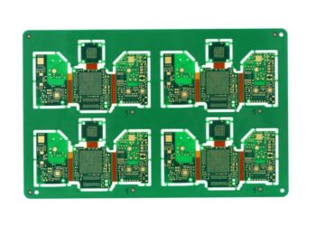
This makes chemical etching ideal for applications such as:
- Lead frames and connector components
- EMI and RFI shielding
- Micro-perforated metal parts
- Precision sensor components
Ideal for Thin and Delicate Metals
Many electronic components are made from thin metal sheets to reduce size and weight. These materials are particularly vulnerable to deformation when processed mechanically.
Chemical etching handles thin metals exceptionally well because:
- No punching or cutting force is applied
- Flatness is preserved across the entire part
- Dimensional accuracy remains stable
This feature is especially critical when working with copper, brass, stainless steel, and nickel alloys which are frequently used in electronics manufacturing.
Material Compatibility for Electronics
Another key advantage of chemical etching is its broad material compatibility. The process supports many metals essential to electronic applications, including:
- Copper and copper alloys for conductivity
- Stainless steel for strength and corrosion resistance
- Nickel and nickel alloys for heat resistance and shielding
- Aluminum for lightweight electronic assemblies
Every material has its own unique reaction to etching chemistry; however, with good process control, manufacturers can produce uniform, high-quality results on a myriad of electronic parts.
Fast Design Iteration Without Tooling Costs
There are short product lifecycles and many design changes in the electronics industry. Traditional tooling processes may hinder innovation and result in additional expenses.
Chemical etching is a tool-free process, which means:
- No hard dies are required
- Design changes are implemented digitally
- Prototypes can be produced quickly
- Scaling to volume does not require retooling
From an engineering and cost point of view, this flexibility also makes the chemical etching process well-suited for both prototype development and large-scale electronics production.
TMNetch Chemical Etching for Electronic Components
For manufacturers seeking reliable, high-precision electronic parts, TMNetch offers specialized chemical etching services tailored to the electronics industry.
TMNetch Capabilities
From a metal fabrication expert’s viewpoint, TMNetch brings together experience, precision, and production efficiency:
- Focused on photochemical etching since 2011
- ISO 9001:2015 certified, ensuring stable and traceable quality
- Extensive experience with electronic-grade metals, including copper, stainless steel, nickel alloys, aluminum, and specialty materials
- Ability to produce fine-feature electronic components with tight tolerances
- Supports thin-gauge materials commonly used in electronics
- Offers rapid prototyping for fast design validation
- Provides secondary processes, such as plating, surface finishing, and forming, to deliver ready-to-use components
Why TMNetch Is a Strong Partner for Electronics
TMNetch chemical etching is particularly well suited for:
- Lead frames and connector components
- EMI and RFI shielding parts
- Precision contacts and terminals
- Custom etched components for sensors and electronic assemblies
With chemical etching and controlled finishing processes, TMNetch offers electronics producers the ability to obtain repeatable performance, high yields and efficient manufacturing.
Chemical Etching vs. Other Manufacturing Methods
From the viewpoint of manufacturing strategy, it is not implied that chemical etching should replace all other processes. However, for parts that need to be precise, made from thin material, and have clean edges, it is frequently better than other options like stamping or laser cutting.
Key advantages include:
- No burrs or heat-affected zones
- Better performance on thin metals
- Lower upfront costs for complex designs
- Faster time to market
These benefits explain why chemical etching remains a preferred process across the electronics industry.
Conclusion
The ability of chemical etching to deliver on precision, reliability and scalability makes it an excellent choice for electronic parts. The process is said to enable design freedom and high‐volume production because it removes mechanical stress, retains material properties, and allows complex shapes while supporting both product innovation and mass production.
For manufacturers looking to optimise electronic component fabrication, partnering with experienced providers like TMNetch chemical etching offers a practical path to high-quality, high-performance results. As electronics continue to evolve, chemical etching will remain a cornerstone technology in precision metal manufacturing.


